 |
| Source |
we increase the capacity of [optical data storage] to the petabit level by extending the planar recording architecture to three dimensions with hundreds of layers, meanwhile breaking the optical diffraction limit barrier of the recorded spots. We develop an optical recording medium based on a photoresist film doped with aggregation-induced emission dye, which can be optically stimulated by femtosecond laser beams. This film is highly transparent and uniform, and the aggregation-induced emission phenomenon provides the storage mechanism. It can also be inhibited by another deactivating beam, resulting in a recording spot with a super-resolution scale. This technology makes it possible to achieve exabit-level storage by stacking nanoscale disks into arrays, which is essential in big data centres with limited space.Below the fold I discuss this technology.
What the authors mean by "petabit level" is:
The ODS has a capacity of up to 1.6 Pb for a DVD-sized disk area through the recording of 100 layers on both sides of our ultrathin single disk.1.6 petabit is 200TB per disk, which is 2,000 times the capacity of triple-level Blu-ray media. So this is a big increase. But weirdly, the caption to their Figure 1 claims that:
The capacity of a single 3D nanoscale disk is approximately equivalent to that of a petabit-level Blu-ray library (15.2 Pb, DA-BH7010, Hualu, China) or an HDD data array (12.64 Pb, EMC PowerVault ME5084, Dell, USA).A decade ago, Facebook's Blu-ray library put 10,000 100GB disks in a single rack for 1 Petabyte or 8 Petabit capacity. This is 5 times as much as the authors' claim for a single disk. The caption's claim of 15.2Pb for the DA-BH7010 is 9.5 times their claim of the capacity of a single disk. Note also that they compare the volume of a single disk to the volume of complete read-write systems, which is comparing apples to oranges. I guess if your meaning of "approximately" is "within an order of magnitude" that makes sense.
 |
| Figure 3a |
The transition from the second to the third state is initiated by the 515-nm femtosecond Gaussian-shaped laser beam and deactivated by the 639-nm CW doughnut-shaped laser beam.
 |
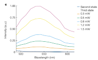
| Figure 3c |
There are a number of reasons to be less enthusiastic about the potential of this technology than Hossenfelder. It is true that they have demonstrated the ability to read and write petabit-scale data on a CD-sized medium. To do the reading they use two lasers, a 480nm pulsed and a 592nm continuous laser. To do the writing they used two lasers, a 515nm femtosecond laser and a 639nm continuous-wave laser. I haven't been able to find a price for a 515nm femtosecond laser, but here is a 1550nm femtosecond laser for $48,880. The femtosecond laser they actually (Acculasers ACL-AFS-515-CUS) used is a substantial box with fans and an AC power input.
The authors make claims of the density of the medium but not of the system. Clearly, current femtosecond lasers are too expensive and too large to use in equivalents of the decade-old Facebook Blu-Ray technology. Something like Microsoft Research's system that uses femtosecond lasers to write in Silica allows the cost of the lasers to be amortized over an entire data-center aisle of media. If you are going to build something like this, there is no reason to use the CD form factor.
The repetition rate of the femtosecond laser was 42MHz. I believe it writes one bit per pulse, so the write bandwidth is limited to around 5MB/sec, meaning that writing an entire disk would take around
the development of next-generation industry-oriented nanoscale ODS that is much less expensive than state-of-the-art optical disk libraries and HDD data arrays will fulfil the vast data storage requirements of the big-data era.It would have similar product issues to those I outlined in Microsoft's Archival Storage Research:
Six years ago I wrote:Hossenfelder makes several mistakes in her report:
time-scales in the storage industry are long. Disk is a 60-year-old technology, tape is at least 65 years old, CDs are 35 years old, flash is 30 years old and has yet to impact bulk data storage.Six years on flash has finally impacted the bulk storage market, but it isn't predicted to ship as many bits as hard disks for another four years, when it will be a 40-year-old technology. Actual demonstrations of DNA storage are only 12 years old, and similar demonstrations of silica media are 15 years old. History suggests it will be decades before these technologies impact the storage market.
Source
- "new disk memory that could bring disk memory into the Petabyte range" - no, that is the Petabit range.
- Optical disks "were outcompeted by hard disks". - no, write-once removable media and on-line storage are two completely different markets. Optical disks lost out to the cloud and to a lesser extent by flash.
- "the information density on compact disks or any optical storage is ultimately limited by the frequency of the laser light" - well yes, but she is talking about a paper describing a 2000-times increase in capacity using laser light.
- "in modern flash drives the information is stored in little magnetizable cells that are a few atoms in size" - no, flash isn't a magnetic technology. She also misses that modern flash is a volumetric not a planar technology, just like the technology in the paper.
- "figured out how to write data in multiple layers" - no, Blu-ray is a multi-layer technology more than a decade old. They figured out how to write a lot more layers of much smaller bits.
- "this could work up to hundreds of layers" - well, they only demonstrated 100 layers, so hundreds plural is speculation. To get to the petabyte range needs at least 500 layers or much smaller bits. Note that modern flash has over 100 layers.

Interesting post. I think you made a calculation error, though. Filling a 200TB disk at 5MB/s would take roughly 11000 hours, not 10,5.
ReplyDeleteThanks, Nikolaj! I fixed it.
ReplyDeleteI'm grateful to the primary author for pointing me to 3D direct laser writing of Petabyte Optical Disk by Eugen Pavel et al from nine years ago. It shows how unlikely it is that the technology Hossenfelder touted will impact the market any time soon. It claims:
ReplyDelete"We report novel results for 3D recording of an optical disk with ultra-high density. Multilayer 5 nm nanomarks were experimentally obtained by using fluorescent photosensitive glass-ceramics and an optical head with λ=650 nm and NA=0.60. The distance between adjacent 5 nm nanomarks has been reduced to 10 nm. Ultra-high density optical data is recorded by focusing laser beam of a CW laser diode operating at low power (Pmax=10 mW)."
This represents a disk capacity of over a Petabyte. While the team wrote at a Petabyte density, they did not read it back. The paper describes how they confirmed the writing using a Tunneling Electron Microscope:
"Detailed analysis of line formation during laser writing was accomplished by TEM measurements. For TEM examination, glass specimens were prepared by sawing, mechanical grinding, polishing and ion milling.The samples were shaped into 3 mm diameter disks using an ultrasonic disk cutter. In order to achieve the desired thickness of a TEM sample, a dimpling grinder was used to thin some more to a thickness of 80 μm, with two parallel faces. Also by using the dimpling grinder the sample was ground to achieve a concavity on both faces of the 3 mm disk until the thickness in the center of the sample was no more than 10 μm. The final step in preparation of the sample for TEM observation is ion milling using a low angle ion milling and polishing system. The ion milling was carried out until the sample was fully perforated by ions."
This comment has been removed by the author.
ReplyDeleteLaura Dobberstein reports that Chinese boffins find way to use diamonds as super-dense and durable storage medium:
ReplyDelete"Researchers at China's University of Science and Technology published research this week in which they detail how they achieved record-breaking storage density of 1.85 terabytes per cubic centimeter by encoding information in diamonds.
To put it in context, advanced hard disk drives can achieve around one terabyte per cubic centimeter, although higher densities have been reported. Enterprise HDDs can last up to a decade. Blu-ray discs, which have similar storage density, can last longer. According to USTC, its technique for encoding data in diamonds produces both greater density and vastly greater durability."
The paper is here.